






日赚4億の「中国のSKハイニックス」、アップルも買い求めている


- 核心ポイント:長鑫存儲は世界第4位のDRAMメーカーとしてまもなく科創板(STAR Market)に上場する。奇夢達(Qimonda)の技術遺産と合肥市政府の支援を背景に、2026年のDRAMスーパーサイクルで驚異的な収益反転を実現し、半年で9年分の累積損失を一掃したが、その収益は主に業界サイクルに依存しており、構造的な優位性によるものではない。
- 主要要素:
- 長鑫存儲の2026年第1四半期の売上高は508億元、純利益は330億元で、1日あたり約4億元の利益を計上。その収益性は貴州茅台(マオタイ)を凌駕し、市場ではA株時価総額トップを目指すとの見方もある。
- 同社は2016年に設立され、奇夢達の技術ファイル(2.8TBのデータ)と約25億ドルを投じた再設計を基に、中国初の自主DRAMとして19nm DDR4の量産化に成功した。
- 2025年末時点での累積損失は366.5億元だったが、2026年第1四半期の純利益は330億元に達し、半年で黒字転換し、長年の損失を補填した。これは主にDRAM価格サイクル(契約価格が前期比93%~98%上昇)によるものである。
- 顧客にはアップル、グーグル、テンセント(200億元超の供給契約)、アリババクラウド、バイトダンスなど国内外の大手企業が名を連ねており、市場での認知度が急速に高まっていることを示している。
- IPOでは295億元の資金調達を予定しており、これは科創板で最大級の調達額の一つとなる。資金は後工程の技術アップグレードや新規プロジェクトに投じられ、評価額は1584億元とされているが、機関投資家の間では時価総額が3~4兆円に達する可能性があるとの見方もある。
Original author: Jialiu
When it comes to the global storage industry, many people only know Samsung, SK Hynix, and Micron. However, many are unaware that the world's fourth-largest player is a Chinese company that hasn't yet gone public, named Changxin Memory Technologies (CXMT).
On July 9, Changxin Technology updated its latest IPO prospectus for the STAR Market. Timing-wise, subscription begins on July 16, payment is due on the 20th, and trading on the STAR Market could potentially start as early as the end of the month.
China's strongest storage leader is arriving by the end of the month.
Data shows that its estimated Q1 2026 revenue is 50.8 billion yuan, a year-over-year increase of 719%. Net profit is 33 billion yuan. Earning nearly 4 billion yuan a day, its profitability surpasses Kweichow Moutai, and the market gives it a trillion-yuan valuation, potentially challenging for the top spot in A-share market value.
As of the end of 2025, the company's accumulated losses were still 36.65 billion yuan.
In other words, Changxin Memory recouped nine years of losses in just half a year. This domestically produced chip company, which had been losing money for nearly a decade, suddenly became one of the most profitable hard-tech enterprises in A-shares.
Over the past week, the name Changxin Memory has frequently appeared in global tech media. Apple is lobbying the US government for a special license, planning to include Changxin Memory in the memory supply chain for Macs and iPads. Google has also initiated procurement evaluations for Changxin's DRAM. Other reports mention that HP and Dell are validating Changxin's DRAM, while Acer and ASUS are asking Chinese partners to use more domestic memory chips. The same week, Reuters reported that Tencent signed a long-term server DRAM supply agreement with Changxin Memory worth over 20 billion yuan, lasting three to five years. Changxin’s prospectus also lists Alibaba Cloud, ByteDance, Lenovo, Xiaomi, OPPO, vivo, and Honor among its clients.
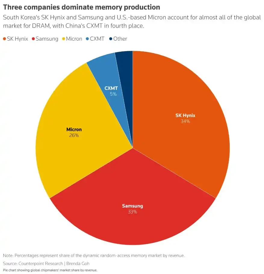
Leading companies in the global memory production field, Changxin's share ranks fourth globally, behind Hynix, Samsung, and Micron. Source: Reuters
Suddenly, Changxin Memory has become a favorite among almost all major domestic and international companies.
How did Changxin go from zero to fourth in the world? How much of its current earnings are due to strength versus luck? Can its trillion-yuan valuation stand firm?
The Road Ahead for Changxin Memory: GigaDevice
The origin story of Changxin Memory must start with why China has always lacked DRAM.
There are many types of memory chips. NAND Flash retains data when power is off, used in phone storage, SSDs, and USB drives. DRAM is runtime memory; data is lost on power loss, but it's fast, serving as the workbench next to CPUs, GPUs, phone SoCs, and AI accelerator cards.
NAND and DRAM are both commodity semiconductors, but DRAM is more like a high-precision steel mill combined with advanced manufacturing. Each generation of process technology must push capacitors, transistors, word lines, and bit lines to their limits, replicating billions of highly consistent units on a single wafer. A slight flaw drops yields and skyrockets costs. When costs explode during a memory downturn, money flows out like water.
That's why the DRAM market eventually boiled down to three giants: Samsung, SK Hynix, and Micron. You can't just join this table with "I have a tech team"; you must survive price wars, capacity wars, patent wars, equipment restrictions, and customer qualifications over a decade or more.
Changxin Memory started around 2016, landing in Hefei. Its key figure is Zhu Yiming.
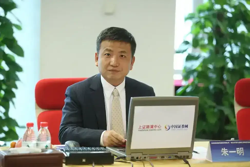
Photo of Zhu Yiming from a meeting
The name Zhu Yiming is not unfamiliar in China's semiconductor circle.
Born in 1972, Zhu Yiming was a child prodigy, entering Tsinghua University's Physics Department at 17. Although studying physics, he excelled at programming, earning over 300,000 yuan annually by writing programs for other companies in the late 1990s. During this work, he learned that chips were designed in the US at the time. Believing chips involved higher technology, he went to the US to study electronic engineering and worked in Silicon Valley after graduation.
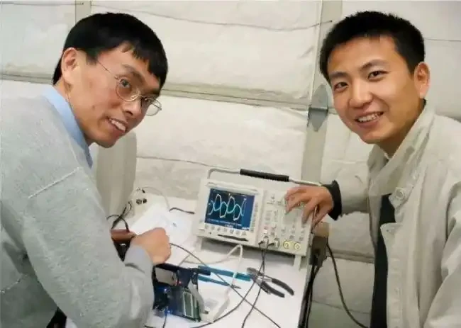
Early photo of Zhu Yiming (right)
In Silicon Valley, Zhu Yiming noticed that the memory industry had shifted from the US to Japan, then to South Korea and Taiwan, China. He estimated that mainland China might also have a significant opportunity, potentially giving birth to a "Chinese version of Samsung." He designed an SRAM (Static Random-Access Memory) chip and returned to China in 2005 to found a company called GigaDevice.
From its inception, GigaDevice was a pure design house, not manufacturing chips itself; all wafer fabrication was outsourced to foundries. Its main products were NOR Flash (memory chips used for router and game console boot programs) and MCUs (microcontrollers for refrigerators and washing machines). Zhu Yiming led the team to create China's first static memory and IP technology, first serial flash product, and first 32-bit general MCU based on the ARM Cortex-M3 architecture. By its IPO in August 2016, it was the largest code flash memory chip design company in mainland China, with revenue growing from 1.489 billion yuan at IPO to 9.203 billion yuan.
Asset-light, high-margin, no need to build its own factories. This was the smartest survival strategy for China's IC design industry at the time.
But this model had a prerequisite: ample foundry capacity and stable prices. In the second half of 2020, Zhu Yiming encountered a hurdle. SMIC's 8-inch capacity became extremely tight, forcing GigaDevice to shift some NOR Flash orders to Hua Hong Semiconductor's 12-inch fab, incurring higher foundry costs. Gross margin in Q4 2020 plummeted from a stable level above 37% to 29.49%. The consequence of tight foundry capacity was directly reflected in the income statement for the first time.
Around the same time, GigaDevice was paying for another acquisition. In 2019, it acquired Shanghai Silead for 1.7 billion yuan, a 16x premium, generating 1.305 billion yuan in goodwill. Silead made under-display fingerprint chips. Zhu Yiming aimed to combine memory, controllers, and sensors to form a platform-type design company. However, Goodix sued Silead for patent infringement, and a price war ensued. Silead only fulfilled 58% of its three-year performance commitment. From 2020 to 2023, GigaDevice took goodwill impairment charges for Silead for four consecutive years, totaling approximately 900 million yuan, eroding most of the 1.3 billion yuan goodwill. The strategy of acquiring another design company to expand product categories also proved untenable.
Zhu Yiming's lesson from these two events was: The ceiling for an asset-light design company isn't design capability, but capacity. And the main battlefield for memory chips isn't NOR Flash, a category occupying only 2.5% of the global market; it's DRAM. But DRAM can't be entrusted to general-purpose foundries like NOR Flash. DRAM processes are highly proprietary; each manufacturer's cell structure, capacitor design, and word line process are customized. Samsung, SK Hynix, and Micron all operate with an integrated design and manufacturing model. To make DRAM, there was only one path: Build your own factory.
This is the background and reason for the birth of Changxin Memory.
Hefei's Third Big Bet, After BOE and NIO
GigaDevice's financials and shareholder structure couldn't support the investment scale for a DRAM fab. After all, Phase 1 required 18 billion yuan, with total investment exceeding 100 billion yuan, and nearly a decade of continuous losses. This money had to come from a different kind of capital.
In 2016, the Hefei government extended an olive branch.
The market often calls Hefei "the city best at venture capital." Hefei's most famous venture capital success story is BOE. The starting point for the world's largest LCD panel shipper, with annual revenue exceeding 200 billion yuan and Chinese panel makers holding 70% of the global LCD market, was in Hefei.
In September 2008, BOE signed a 6th-generation line investment framework agreement with Hefei. The project's total investment was 17.5 billion yuan. The registered capital of 6 billion yuan was contributed by the Hefei side, injected via a BOE private placement, and then fully invested in the project company. Instead of just giving BOE a subsidy, Hefei used local government platforms to take a controlling stake, provide bridging funds, loan interest subsidies, and land and energy support, shouldering BOE's most difficult construction period. By clustering around BOE, Hefei attracted glass substrates, polarizers, driver chips, and equipment materials, gaining the city label "Capital of New Display."
The second typical story is NIO. In April 2020, NIO had just crawled out from the brink of death in 2019. Hefei Construction Investment and Anhui Emerging Industry Investment injected a total of 7 billion yuan in cash into NIO China. NIO China's headquarters landed in the Hefei Economic and Technological Development Zone. NIO later became one of the representative brands of China's high-end electric vehicles, with a market cap once exceeding 100 billion USD.
Find an asset-heavy industry leader, use transaction structures instead of simple subsidies, help the company get through the construction phase, and then use the leader to attract upstream and downstream industries to take root locally.
In 2016, Hefei used the same investment logic for its next big bet.
Yuan Fei, an early key figure at Hefei Industrial Investment, later said, "Whether from Hefei Industrial Investment or the industry side, everyone involved early in Changxin bore unprecedented risk and pressure."
After all, DRAM is harder than display panels or complete vehicles, with higher risks related to technology, equipment, yields, patents, and export controls. But from a local industrial organization perspective, like BOE and NIO, it devours money in the short term. However, if successful in the long run, it would significantly reshape the supply-demand relationship of an entire industrial chain.
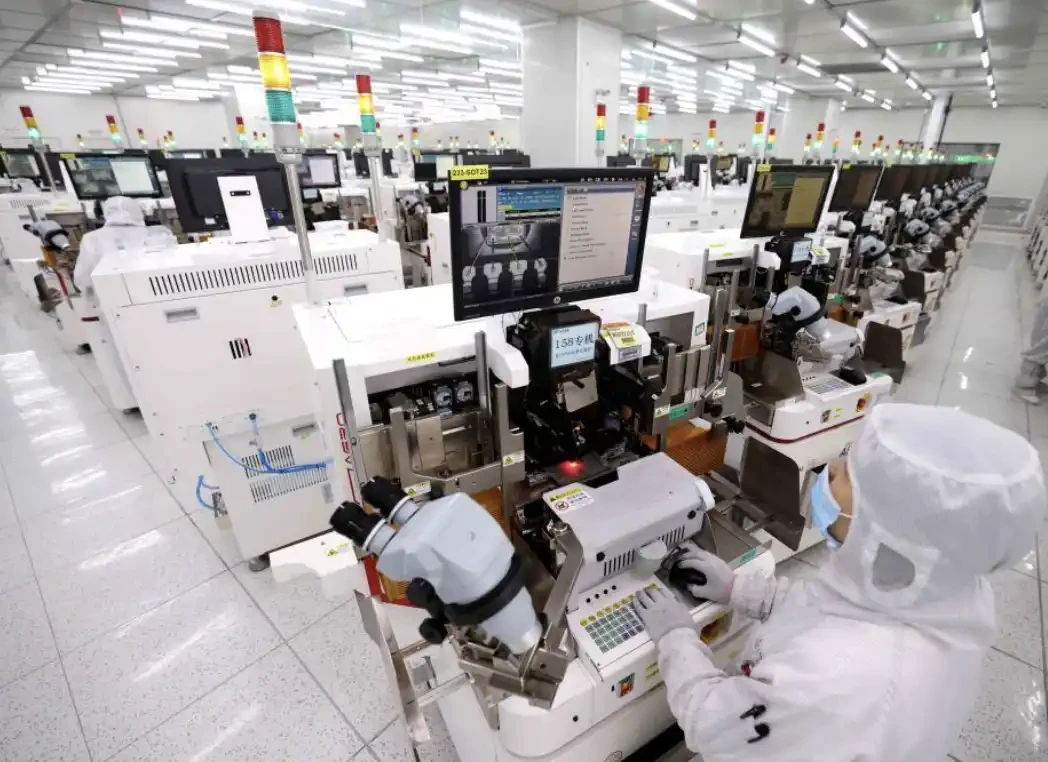
Anhui Hefei promotes the integrated circuit industry
Hefei Industrial Investment contributed 14.4 billion yuan in Changxin Memory's first phase alone, with the project's total investment exceeding 100 billion yuan.
In July 2018, GigaDevice announced: Zhu Yiming resigned as General Manager, retaining only the Chairman role, and formally became Chairman and CEO of Changxin Memory. The industry called this Zhu Yiming's "second startup."
The current shareholder list already reveals the landscape of this gamble. The top five shareholders are Qinghui Jidian at 21.67% (fully controlled by Hefei state-owned assets), Changxin Jicheng at 11.71%, Phase II of the Big Fund at 8.73%, Hefei Jixin at 8.37%, and Anhui Investment at 7.91%. Hefei state-owned assets hold a combined stake of over 36%.
Among other shareholders, Alibaba Cloud holds 3.85% (61 billion yuan investment, implying a 158.4 billion yuan valuation), and GigaDevice holds 1.8%. The investor list also includes the State-owned Enterprise Reform Fund, CICC Capital, Legend Capital, China Merchants Capital, Yunfeng Capital, Tencent, and Alibaba.
The money and momentum were in place. But Zhu Yiming's "second startup" still lacked one thing: core technology.
The Technological Legacy of a Bankrupt German Company
Around 2016, the three giants Samsung, SK Hynix, and Micron collectively controlled over 90% of the global DRAM market share, the result of a decade-plus elimination game.
The DRAM industry has killed off players every few years since the 1980s.
Japan once held over 80% of global DRAM production capacity, but by the 2010s, only Elpida was left struggling, eventually acquired by Micron in 2012. Europe once had Qimonda, under Infineon, but it went bankrupt in 2009.
Zhu Yiming's solution was hidden within this German company that had already gone bankrupt in 2009.
The name Qimonda comes from two words. "Qi" is Chinese for "energy," flowing power. "monda" is Latin for "world." The literal meaning: the key to opening the world.
A beautiful name. The company's fate was tragic.
Qimonda was spun off from its parent company Infineon in May 2006 and listed on the NYSE on August 9, 2006, under the ticker QI. Upon listing, it was already a major global supplier of memory products and a leader in 300mm wafer manufacturing technology. By 2008, Qimonda had completed development of a 46nm stack process product based on Buried Word Line, offering 100% more capacity than the previous 58nm process, just short of mass production.
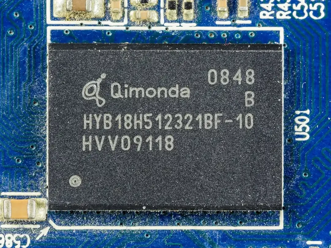
Image of Qimonda DDR2/GDDR chip products
But the financial crisis hit. DRAM prices fell off a cliff. Samsung expanded production at a loss to pressure competitors. Qimonda's new technology wasn't ready for mass production before its funding dried up. It filed for bankruptcy in 2009. The lights went out for Europe's last major memory maker. The Munich R&D center emptied, its 12,000 employees scattered, absorbed by Samsung, Micron, and SK Hynix. In 2012, Qimonda's bankruptcy trustee began selling its 7,500 patents.
Zhu Yiming saw his opportunity in this history.
Qimonda died from the cycle, not from its technology. It left behind 2.8TB of technical documents and tens of thousands of patents, a legacy buried for nearly a decade. In the DRAM products of today's Samsung, Micron, and SK Hynix, one can actually find shadows of Qimonda's buried word line and honeycomb capacitor structures, which indirectly flowed into the process systems of the big three through partners like Inotera and Winbond.
But how to acquire this legacy and use it to build a factory was a huge problem, with a bloody lesson ahead.
2016 was considered the "first year" of the memory resurgence in China. Before that, China's DRAM industry had completely declined, facing technology monopolies from US and Korean companies with no ability to fight back.
When China launched its national memory team, besides Changxin, there were two other parallel paths: Yangtze Memory Technologies (YMTC) for NAND Flash and Fujian Jinhua Integrated Circuit (Jinhua) for DRAM.
In 2017, Micron sued UMC and Jinhua simultaneously in the US and Taiwan, alleging that three employees who moved from Micron to UMC stole Micron's DRAM trade secrets, with one person accused of stealing over 900 technical documents. In October 2018, the US Department of Commerce added Fujian Jinhua to the Entity List for national security reasons, imposing export controls. UMC immediately announced it would suspend technical cooperation with Jinhua. Equipment supply was cut off, technical cooperation was frozen, and the project stalled. The US Department of Justice also filed a criminal lawsuit against Jinhua and UMC, accusing them of economic espionage, facing potential fines exceeding 20 billion USD. It wasn't until the end of 2023 that Micron and Jinhua reached a global settlement, ending a dispute that lasted six years.
The lesson from Fujian Jinhua was clear: Getting involved in a trade secret dispute with Micron leads to being placed on the Entity List, equipment cutoffs, and project suspension. If a new DRAM company hits a landmine in intellectual property, commercial customers won't dare to use it, equipment suppliers won't dare to supply it, and the international market will be dragged down by lawsuits.
So, when Qimonda's bankruptcy trustee began selling its 7,500 patents, Zhu Yiming quickly moved. He acquired over ten million DRAM technical documents (about 2.8TB of data), which already included 16,000 patent applications. Subsequently, he spent approximately 2.5 billion USD on a comprehensive redesign of the original architecture, advancing Qimonda's 46nm process to the 10nm class. He also signed patent license agreements with Wi


