




NVIDIA罕見「掉鏈子」:主力產品延期一年,AMD和Google迎來窗口期


- 核心觀點:NVIDIA 基於 Rubin Ultra 架構的 Kyber NVL144 機架,因核心部件 PCB 中板製造工藝極端困難,延遲超過 12 個月至 2028 年。其過渡方案 NVL72x2 也已因客戶反對取消,同時 NVL576 系統同樣面臨 CPO 技術挑戰,導致 NVIDIA 在規模擴展領域出現階段性空白,為競爭對手創造機會。
- 關鍵要素:
- Kyber NVL144 延遲的直接原因是 PCB 中板(正交背板)的製造難題。該板採用 78 層 M9 級覆銅板 + 石英布 + PTFE 混合材料,線寬與線距 ≤ 25μm,以實現 448G+ SerDes 速率。
- NVIDIA 曾開發的 NVL72x2 過渡方案,因雲服務商和超大規模數據中心運營商反對其「奇特設計和繁重運維負擔」而遭取消,兩條路線均受阻。
- NVL576 系統透過 CPO 連接 8 個 Oberon 機架,但 CPO 當前正面臨挑戰。SemiAnalysis 稱其可能延遲或僅限小批量出貨,量產成熟度存疑。
- 4 計算晶片版的 Rubin Ultra 已被取消,僅保留 2 晶片版本,單機架算力上限大幅下調。NVIDIA 計劃增加機架銷售以彌補缺口。
- NVIDIA 在 Rubin Ultra 規模擴展領域缺乏經過驗證的方案,這為 AMD MI500X、Google TPUv8i Broadfly 等競爭對手在規模擴展能力上超越它提供了窗口期。
Original Title: "SemiAnalysis Reveals Another Pre-Market Bomb: NVIDIA's Kyber NVL144 Rack Delayed Over 12 Months Due to 'PCB Midplane Manufacturing Difficulties'"
Author: Long Yue
Source: Wall Street News
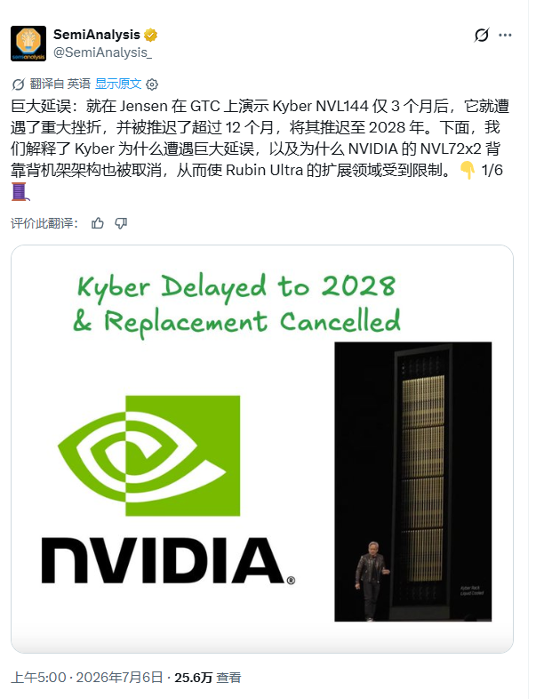
On the morning of July 6, semiconductor industry research firm SemiAnalysis published six consecutive tweets on X (formerly Twitter), disclosing significant delays and multiple cancellations for NVIDIA's Kyber NVL144 rack architecture. The news drew market attention before the market opened.
SemiAnalysis stated bluntly: "Major Delay: Just three months after Jensen Huang showcased the Kyber NVL144 at GTC, the product has suffered a major setback, delayed by over 12 months to 2028."
The PCB Midplane: The Board Holding Back Kyber
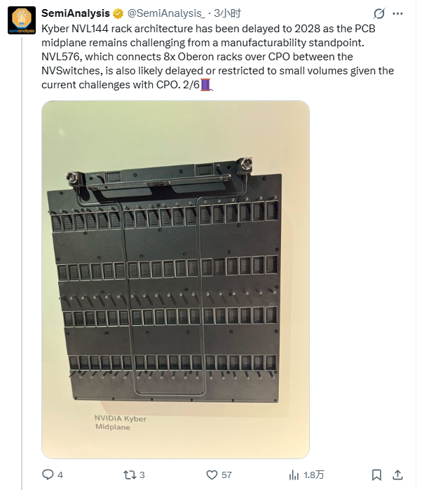
SemiAnalysis suggests the direct cause of the Kyber NVL144 delay points to a critical hardware component—the PCB Midplane, officially referred to by NVIDIA as the "Orthogonal Backplane."
The firm stated: "The Kyber NVL144 rack architecture has been delayed to 2028 because the PCB midplane still faces significant manufacturing challenges. The NVL576, which connects 8x Oberon racks via CPO between NVSwitches, is also likely delayed or limited to small-volume production due to current CPO challenges."
The gray board Jensen Huang displayed at the GTC conference in March was precisely the orthogonal backplane for the Rubin Ultra (Kyber architecture) cabinet. Its function is to achieve a 90° vertical interconnection between the compute trays and the switch trays—compute trays connect vertically, enabling direct board-to-board connection with the rear switch trays via this midplane, completely eliminating traditional cable clutter.
This board is extremely difficult to manufacture. According to the technical analysis, the backplane uses M9-grade copper-clad laminate + quartz fabric (Q fabric) + PTFE hybrid materials, with 78 layers (formed by laminating three 26-layer boards) and a line width/spacing of ≤25μm, meeting the ultra-high-speed signal integrity requirements of 448G+ SerDes rates.
Why is this board a necessity? According to the technical analysis, the Rubin Ultra NVL144 rack needs to connect 144 GPUs in a single domain. Using traditional copper cabling would require over 20,000 cables, increasing weight by more than 30% and causing severe signal degradation. The orthogonal backplane is one of the few viable solutions under current technological constraints.
Alternative NVL72x2 Plan Also Canceled
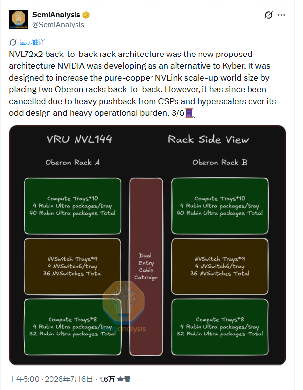
Faced with Kyber's manufacturing difficulties, NVIDIA attempted to develop a transitional solution—the NVL72x2 back-to-back rack architecture.
According to SemiAnalysis, the design concept involved placing two Oberon racks back-to-back and expanding the scale domain via pure copper NVLink, thus bypassing the manufacturing challenges of the Kyber midplane.
However, this plan ultimately failed to materialize. SemiAnalysis stated that NVL72x2 "was canceled due to strong opposition from cloud service providers and hyperscaler data center operators regarding its peculiar design and heavy operational burden."
With both paths blocked, NVIDIA faces a temporary gap in scaling the Rubin Ultra.
NVL576 Also Under Pressure, CPO Challenges Cannot Be Ignored
The Kyber NVL144 isn't the only product delayed. SemiAnalysis also pointed out that NVL576—an even larger system connecting 8 Oberon racks via CPO (Co-Packaged Optics)—"given the current challenges facing CPO, may also be delayed or limited to small shipments."
CPO is the optical interconnect technology NVIDIA is introducing for the first time in the scale expansion network during the Rubin Ultra phase. According to SemiAnalysis's research report from March 2026, NVL576's design strategy was: maintain copper cabling expansion within the rack and connect NVSwitches between racks via CPO, forming a two-tier fully interconnected network.
However, the manufacturing maturity of CPO itself remains a variable. In its report, SemiAnalysis explicitly noted that CPO NVSwitch will not be fully ready until the Feynman generation.
Rubin Ultra Itself Also Scaled Down: 4-Chip Version Canceled
Alongside the delay news, a significant product-level change was also disclosed.
SemiAnalysis stated that the 4-compute-chip version of Rubin Ultra has been canceled, "retaining only the smaller 2-compute-chip version of Rubin Ultra, whose actual performance is roughly half of the 4-chip version."
This means that even if the Kyber rack is eventually delivered on schedule, the compute ceiling per rack has been significantly lowered.
In response, SemiAnalysis noted that NVIDIA will "compensate for this shortfall by significantly increasing the sales of Oberon Rubin racks and Oberon Rubin Ultra racks."

Competitive Window: AMD and Google May Benefit
The gap in the scale expansion domain directly impacts NVIDIA's competitive position in large-scale training scenarios.
SemiAnalysis pointed out: "NVIDIA currently has no verified solution to expand the scale domain of Rubin Ultra, leaving room for competitors like AMD MI500X or TPUv8i Broadfly to surpass Rubin Ultra in scale expansion capabilities."
According to NVIDIA's current roadmap, CPO NVSwitch will not appear until the next-generation Feynman platform. Until then, the scale expansion ceiling for Rubin Ultra is constrained.
At the end of the tweet thread, SemiAnalysis indicated that these delays and cancellations have implications for the memory, PCB, and ODM supply chains.
The manufacturing challenge of the Kyber midplane directly points to the technological bottleneck of high-end PCB suppliers. The required 78-layer ultra-high-density PCB, M9-grade copper-clad laminate, and PTFE hybrid materials represent the current limits of PCB manufacturing technology.